
Delay-Locked Loops
DDR DLL
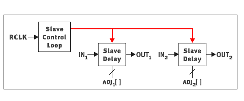
The DDR DLL uses a reference clock to establish a time base in order to delay arbitrary (nonperiodic) strobe signals by precise fractions of the clock cycle. It uses a phase-locked analog delay line which rejects temperature and supply voltage variations, and has high supply noise rejection for very low jitter operation. TCI can configure this block to have almost any number of slaves (which delay the arbitrary signals) with a single master section (which establishes the time base) to minimize area and power. The slave delays can be independently set to precise values or dynamically adjusted after determining the boundaries of a data eye. The DDR DLL has excellent linearity and very high resolution. TCI can also configure this block to output multi-phase clocks directly from the reference clock.
The analog delay-line architecture used in our DLL design sharply contrasts with those used in digital DLL approaches. The analog control loop allows our DLL to continuously and smoothly compensate its delays to changing voltage and temperature conditions, without any quantization jitter or output glitches. However, digital delay-line control loops, which typically multiplex between inverter outputs along a string of inverters, must select between quantized delay values. Such approaches can lead to imprecise delays and either output glitches from updates or timing drifts from voltage and temperature variations in the absence of updates. The analog delay line used in our DLL design is internally isolated from supply noise for very low output jitter, while digital delay lines tend to be very supply noise sensitive as they convert it percent-for-percent into output jitter. Our analog delay line also provides pulse width compensation to minimize pulse width distortion, unlike digital delay lines. Finally, our DLL design provides very high digital adjustment resolution (typically 7 bits), where the steps are precise fractions of the clock period, unlike digital DLL designs where the adjustment steps are very large and not well calibrated.
Multi Phase DLL
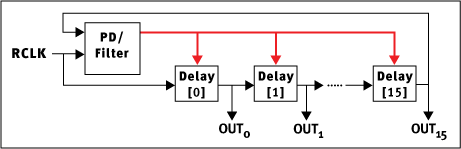
The Multi Phase DLL is designed for high-speed interface applications. The DLL generates precise multi-phase clocks directly from the reference clock. It delivers optimal jitter performance over a wide frequency range. The analog delay-line architecture used in our DLL design is internally isolated from supply noise for very low output jitter. The analog delay line also provides duty cyle correction.