
DDR PHYs
DDR 4/3 PHY
The TCI DDR 4/3 PHY is a high-performance, scalable system using a radically new architecture that continuously and automatically adjusts each pin individually, correcting skew within byte lanes. This state-of-the-art tuning acts independently on each pin, data phase and chip select value. Read data eye and gate timing are also continuously adjusted. Automatic training is included for multi-cycle read gate timing and write leveling, write data eye timing, and internal and external (on DRAM) Vref setting.
Remarkable physical flexibility allows the PHY to adapt to each customer’s die floorplan and package constraints, and is delivered and verified as a single unit for easy timing closure with no assembly required.
The PHY is DFI 3.1 compliant, and when combined with a suitable DDR 4/3 memory controller, a complete and fully-automatic DDR 4/3 system is realized. The PHY is immediately available in the TSMC 28nm HPM/HPC process, with additional TSMC and GLOBALFOUNDRIES processes to follow.

Block Diagram
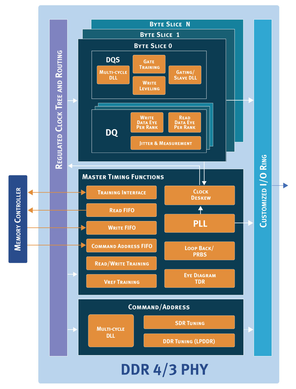
Product Features
- Supports DDR4-2400, DDR3-2133 and LPDDR3-1066, simultaneously with one hard macro
- DFI 3.1 compliant
- Supports x4, x8 and x16 DRAMs
- Up to 144 bits wide
- Up to 4 chip selects
- Includes PLL, with frequency multiplication from low frequency reference
- Per-pin architecture, similar to a SerDes, automatically corrects skew, increases data eye and eliminates most parallel interface problems
- Continuous adjustment of read data eye and gate timing
- Automatic Training includes:
— Multi-cycle read gate training and write leveling
— Write data eye centering
— Internal Vref adjustment
— External Vref adjustment in each DRAM - Localized and optimized PHY-to-memory controller interface to ease timing closure
- Full speed read/write BIST with pseudo-random data, mux-scan ATPG and 1149.1 Boundary Scan
- Circuitry in each pin able to measure the data eye and jitter, and calculate flight delays
Performance Advantages
Tuning for Performance
The PHY has been designed from the ground up to provide extensive, automatic and continuous tuning. Each pin constantly adjusts separate read data eyes for even and odd data phases, taking jitter into account. Tuning is also done separately for each chip select value. Pervasive tuning is the key to performance.
Timing Closure
To make timing closure of the DDR 4/3 PHY to the memory controller faster, the interface from PHY to memory controller is localized and optimized for easy timing.
Automatic Training
DDR4 systems require a great deal of training to function properly. The TCI PHY, combined with an appropriate controller, does all of the required training with almost no user interaction. Low overhead, incremental training can be done at the user’s discretion to achieve even higher data rates.
Automatic training includes multi-cycle read gate training and write leveling, and read and write data eye centering. DDR4 systems require internal Vref and external Vref (on DRAM) adjustment, which the TCI PHY performs automatically using very sophisticated algorithms.
Tools
TCI uses many proprietary tools to achieve a level of quality, flexibility and automation unseen in mixed-signal design, and not currently available in this type of hard IP.
Integration Advantages
No Assembly Required
The PHY is fully tested and verified with state-of-the-art timing analysis. Through a careful, joint process, the I/O ring and package are co-designed prior to PHY delivery, so that the PHY can be fully described, verified and delivered as a whole. Tremendous flexibility is allowed and no assembly is required.
Lower Package and Board Costs
Simpler and cheaper (fewer layer) chip packages and boards can be designed by eliminating the need for matched trace lengths, and by allowing for tremendous flexibility in the I/O ring/package co-development.
By intentionally skewing adjacent pins, lower cost power delivery systems can be used, and wire bond packages can be used at a higher speed.
Measurement Resources for Characterization
The PHY contains many resources that can be set up to quickly characterize a new chip, a package or a customer’s PCB board. Per pin measurements include: DQ switching jitter, read DQS jitter, read data eye, write data eye, Vref sensitivity and flight times. Pin and pattern weaknesses can be found quickly, without expensive lab equipment. Using an appropriate controller, the DDR interface can be fully characterized without CPU interaction.
Test
The PHY includes a full speed read/write BIST, which tests the complete read and write paths of every pin simultaneously with pseudo-random data. The PHY design kits include industry-standard boundary scan chains and all the appropriate views for DFT.